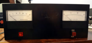
The dead power supply I picked up at the TARC swap meet last year has been sitting in a couple of closets for the past year, and now I’m finally getting around to poking around inside.
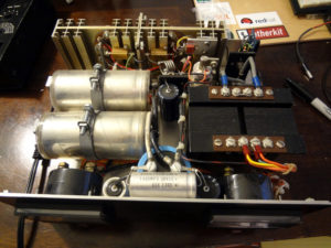
The innards of the power supply look pretty good. Everything looks pretty clean, no scorch marks, and hardly any dust.
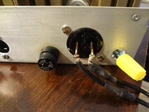
Looking at the back panel doesn’t inspire much confidence though. Looks like at some point someone soldered a regular power cable to the original (I think) AC input and covered it with heat shrink. I might have to do something about that when I start working on the power supply.
So far everything looks in pretty good shape. Not sure what the problem with it is (aside from a blown fuse), but before I dive in and start mucking around, I’m going to see if I can reverse engineer a schematic for the power supply. There aren’t any labels on the power supply so I can’t look anything up. Should be a fun exercise.
Discover more from AB4UG Radioblog
Subscribe to get the latest posts sent to your email.